Overview
One of the primary features of a microprocessor is to interact with and control external devices. These devices may be something as simple as an LED or a push button. In order to interface with such devices, almost all microprocessors have dedicated pins that can be controlled by software. We are going to examine the most basic digital interface: the Input/Output port or IO port.
Construction of an IO Pin
An IO pins is constructed using a combination of both P and N channel MOSFETS.
P-Channel MOSFET
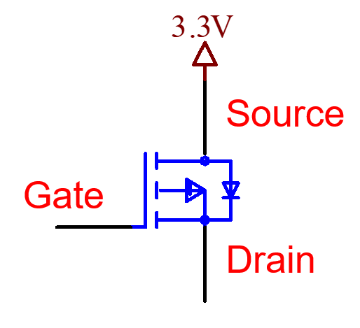
A P-channel MOSFET is a type of field-effect transistor (FET) that acts like an electronically controlled switch. It has three terminals: the Gate (G), Source (S), and Drain (D).
In a P-channel MOSFET, the Source is typically connected to a positive voltage. This terminal supplies voltage to the rest of the circuit when the FET is turned on.
The Gate controls whether the FET is on or off. To turn on a P-channel MOSFET, the voltage at the Gate must be lower than the voltage at the Source—in other words, there must be a negative voltage difference between Gate and Source (VGS < 0). For example, if the Source is at +3.3V, setting the Gate to 0V creates a VGS of -3.3V, which turns the FET on and allows current to flow from Source to Drain.
Conversely, if the Gate is at the same voltage as the Source (e.g., both at +3.3V), then VGS is 0V, and the FET is off. In this state, no current flows from Source to Drain, and the Drain is effectively disconnected from the Source voltage.
N-Channel MOSFET
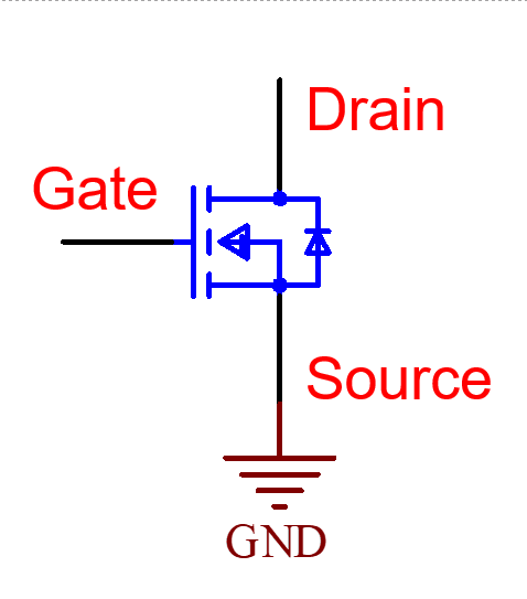
An N-channel MOSFET is very similar to a P-channel MOSFET, but with a key difference: the Source terminal is typically connected to ground (0V) instead of a positive voltage.
Just like with a P-channel device, the Gate controls whether the FET is on or off. However, for an N-channel MOSFET to turn on, the voltage at the Gate must be higher than the voltage at the Source—that is, there must be a positive voltage difference between Gate and Source (VGS > 0). For example, if the Source is at 0V, applying +3.3V to the Gate creates a VGS of +3.3V, which turns the FET on and allows current to flow from Drain to Source.
If the Gate is at 0V (the same as the Source), then VGS is 0V, and the FET is off. In this state, no current flows through the device.
Also, take note of the symbol differences between P-channel and N-channel MOSFETs: the Source terminal is typically drawn on opposite sides in circuit diagrams, reflecting their different voltage roles.
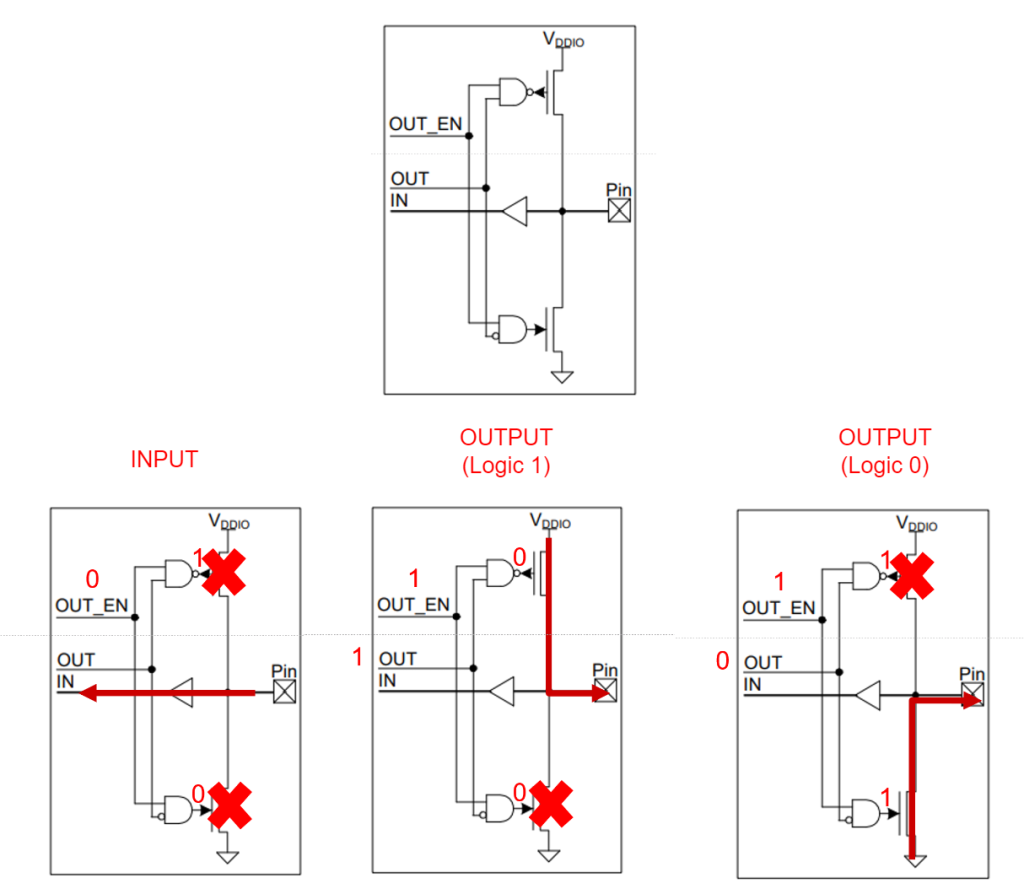
IO Pin Construction Using Complementary MOSFETs
An IO (Input/Output) pin is typically constructed using a P-channel MOSFET paired with an N-channel MOSFET. The Drains of both transistors are connected together in what is commonly referred to as a Totem Pole or Push-Pull configuration.
Each transistor is controlled by its own logic gate—usually two slightly different AND gates—which ensure that the P-channel and N-channel FETs are never on at the same time. This prevents a short circuit between the power supply and ground.
Because an IO pin can operate in either Input or Output mode, there is typically an Output Enable (OE) signal. This signal determines whether the IO pin actively drives a signal (Output mode) or is placed in a high-impedance state (Input mode), allowing external signals to be read without interference.
IO Port Basics
A IO port is a collection of external pins on a microprocessor that can be configured to act as either an input or an output. Voltage levels present on the physical pins are converted into corresponding logic values. The supply voltage of the microprocessor, commonly called VDD, determines what voltage level is equivalent to logic 1. If the supply voltage is 3.3V, an input voltage of 3.3V will be interpreted as logic 1. Similarly, 0.0V will be interpreted as logic 0.
Reading from an Input
When an IO pin is configured as an input, it does not drive a voltage. Instead, it accepts for an external signal that sets the voltage level on the pin.
A push button is a simple electronic component that shorts two terminals together when pressed. Internally, it contains one or more sets of conductive contacts that close the circuit when the button is actuated.
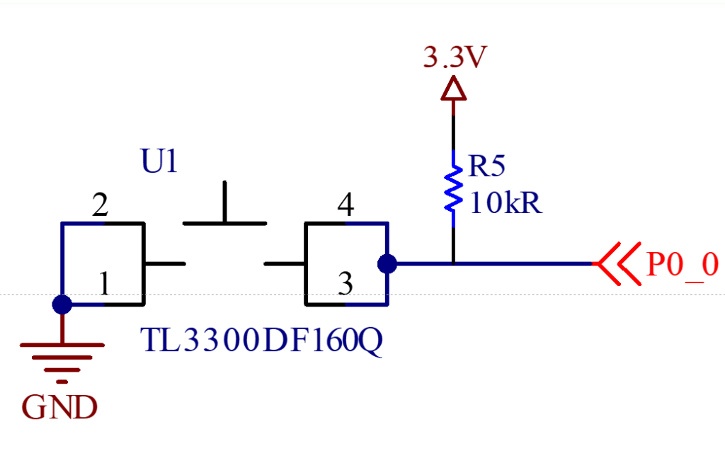
In the example shown, the push button has four pins:
- Pins 1 and 2 are internally connected.
- Pins 3 and 4 are also internally connected.
To use the button with an IO pin:
- One side of the button (e.g., Pins 1 and 2) is connected to ground (GND).
- The other side (Pins 3 and 4) is connected to the IO pin.
When the button is pressed, the internal contacts short the two sides together, creating a path from the IO pin to ground. As a result, the IO pin reads a logic 0 (0V). Since the signal is active when low, this is called an active-low push button.
When the button is not pressed, the IO pin is still connected to Pins 3 and 4, but those pins are not connected to any voltage source. This leaves the IO pin in a floating state, which can lead to unpredictable readings.
To ensure a stable logic level when the button is not pressed, a pull-up resistor is used. This resistor connects the IO pin to a positive voltage (typically 3.3V), pulling the pin high when the button is open. When the button is pressed, the resistor limits the current flow between 3.3V and GND, preventing a short circuit.
Pull-up resistors are commonly used to set a known default value on input pins. Typical values range from 2k? to 100k?, depending on the circuit’s requirements.
Controlling Output Pins
In this example, we have two IO pins, each controlling an LED. The way each LED is turned on depends on how it is wired:
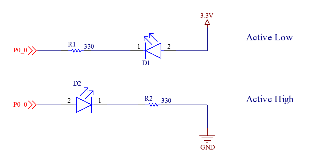
Top LED – Active-Low Configuration
To turn on the top LED, the software must write a logic 0 to the output pin. Here’s why:
-
- The anode of the LED is connected to 3.3V.
- The cathode is connected to the IO pin.
- When the IO pin is set to 0V, a forward voltage drop is created from anode to cathode, allowing current to flow and the LED to light up.
This setup is called an Active-Low LED because the LED turns on when the IO pin is driven low.
Bottom LED – Active-High Configuration
To turn on the bottom LED, the software must write a logic 1 to the output pin:
-
- The cathode is connected to ground through a resistor.
- The anode is connected to the IO pin.
- When the IO pin is set to 3.3V, a forward voltage drop is created across the LED, allowing current to flow from the IO pin to ground.
This is known as an Active-High LED because the LED turns on when the IO pin is driven high.
Current-Limiting Resistor
In both configurations, a resistor is placed in series with the LED to limit the current flowing through it. This protects both the LED and the IO pin from excessive current. The higher the current, the brighter the LED
The current through the LED can be calculated using Ohm’s Law:
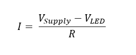
-
- VSUPPLY is the voltage level supplied by the IO pin.
- VLED is the forward voltage drop of the LED, typically 2V for red LEDs.
- R is the resistance in ohms
If we do not use a current-limiting resistor in series with an LED, the circuit allows excessive current to flow through the LED and the IO pin because the denominator is effectively zero (no resistance). This can cause us to exceed the maximum current rating of the IO pin, potentially causing permanent damage to the microcontroller.
Each IO pin has a maximum current sourcing/sinking capability, typically in the range of 10–25 mA depending on the device. Exceeding this limit can lead to degraded performance or permanent damage of the pin.
Using a current-limiting resistor ensures that the current stays within safe limits, protecting both the LED and the IO pin. It also allows you to control the brightness of the LED by adjusting the resistor value.
De-bouncing a Push Button
A common problem encountered when using a push button is that the mechanical contacts of some push buttons will intermittently make contact, or bounce, when first pressed. The image below demonstrates this phenomenon.

If an application were to examine the IO pin in rapid succession, the application might treat a single button press as multiple button presses. In most situation, this is not the behavior that the user would expect.
Hardware Debouncing
In order for the application to detect only a single push button event, we need to de-bounce the button. De-bouncing a push button can be accomplished in hardware using a few different techniques such as a Schmitt triggered input or by adding an resistor-capacitor combination to the input pin.

The voltage on the IO pin cannot change instantaneously due the presence of the capacitor. Choosing the correct R and C values will act to filter out the temporary spikes in voltage due to the bouncing of the button.
Software Debouncing
The most straightforward way to debounce a pushbutton in software is to use a sample-and-delay strategy. This strategy is a non-blocking approach that uses a timer interrupt to sample the button state at regular intervals (e.g., every 10 ms).
Within the interrupt service routine (ISR), the ISR can track how long the button has remained in a stable state by maintaining a counter. If the button is bouncing (the logic value is alternating between 1 and 0), the counter is reset to 0. Once the button state has remained unchanged for a sufficient number of samples—indicating that bouncing has stopped—the ISR can update a global flag or variable to signal that a valid button press or release has occurred.