embedded software for ARM-based microcontrollers. At its core, an embedded application often functions as a control loop that interacts with specific memory-mapped addresses to communicate with both internal peripherals and external devices.
To develop reliable and efficient firmware, engineers must grasp how the high-level code they write interacts with memory resources. This understanding ensures proper use of memory resources including code space, SRAM, and peripheral registers. Without this knowledge, developers risk introducing bugs or performance issues that stem from incorrect assumptions about how memory is organized and accessed.
By understanding the memory map, firmware designers can write code that is not only correct but also optimized for the hardware it runs on—leading to more reliable and maintainable embedded systems.
Code Region
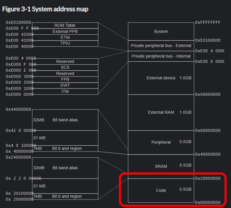
This image illustrates the Cortex-M memory map, showcasing how the 32-bit address space is structured. With 32 address bits, Cortex-M microcontrollers can theoretically access up to 4 GB of memory.
At the bottom of the memory map lies the Code region, typically starting at address 0x00000000. This region is non-volatile, meaning it retains its contents even when power is removed. It is primarily used to store firmware and application code. Since this area is usually mapped to Flash memory, it is read-only during normal operation.
Firmware updates to the Code region are typically performed using debug interfaces such as SWD (Serial Wire Debug) or JTAG, which allow external tools to write new code into Flash memory.
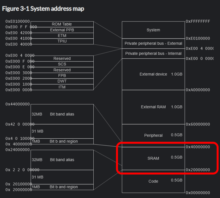
SRAM
Next in the Cortex-M memory map is the SRAM region, which typically begins at address 0x20000000 (twenty million in hexadecimal). This region represents volatile memory that is fully read-write, making it ideal for storing variables, the program stack, and heap during application execution.
Because SRAM is volatile, its contents are lost when power is removed. This makes it suitable for temporary data that only needs to persist while the system is running.
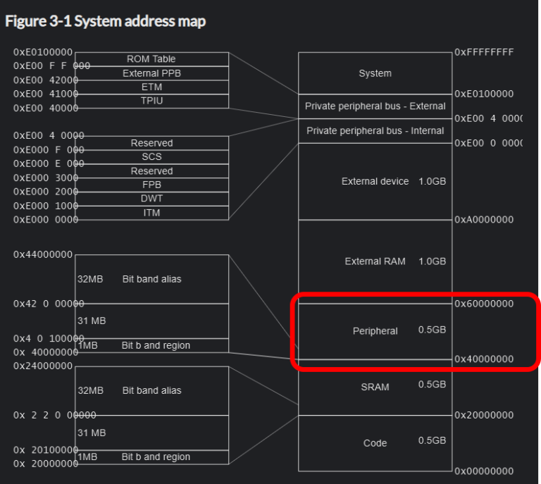
Peripheral Region
Starting at address 0x40000000 (forty million in hexadecimal), we enter the Peripheral region of the Cortex-M memory map. This area is reserved for memory-mapped I/O, allowing software to interact directly with hardware components such as timers, ADCs (Analog-to-Digital Converters), GPIOs (General-Purpose Input/Output), UARTs (Universal Asynchronous Receiver-Transmitters), and more.
By reading from or writing to specific addresses within this region, firmware can control and monitor hardware peripherals. Each peripheral is assigned a unique block of addresses, and the layout is defined by the microcontroller’s manufacturer. This direct access model enables efficient and deterministic control of hardware, which is essential for real-time embedded applications
Although Cortex-M microcontrollers feature a 32-bit address space, which theoretically allows access to 4 GB of memory, it’s important to understand that not all of this space is physically implemented or usable.
For example:
- The Code region might only contain a few hundred kilobytes of Flash memory.
- The SRAM region could range from as little as 8 KB to 256 KB, depending on the specific microcontroller model.
Large portions of the address space are reserved or unused, meaning they do not correspond to any real hardware. Accessing these unused regions typically results in a bus fault or no operation, depending on the system configuration.
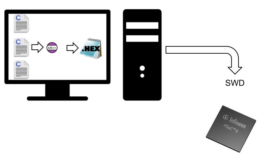
Programming the Code Section
Once the application code is complete, it is compiled using a cross compiler. A cross compiler is a special type of compiler that runs on one architecture—typically the x86 or x64 architecture of your development machine (like a laptop or desktop)—but generates executable code for a different target architecture, such as the ARM Cortex-M microcontroller.
This is necessary because the microcontroller has a completely different instruction set and hardware environment than your development system. The cross compiler translates your C source code into machine code that the microcontroller can execute, producing output files such as:
- ELF files (Executable and Linkable Format) for debugging
- HEX or BIN files for flashing onto the device
The ARM cross compiler generates a HEX file, which contains the ARM machine instructions that implement the application. This file represents the binary code that will be stored in the microcontroller’s Flash memory (i.e., the Code region).
To load this application onto the microcontroller, developers use a serial interface called SWD (Serial Wire Debug). SWD is the standard programming and debugging interface for ARM Cortex-M microcontrollers. It provides a two-wire connection (plus ground) that allows external tools—such as debuggers or programmers—to:
- Flash new firmware into the Code region
- Set breakpoints and step through code
- Inspect and modify memory and registers
Once the HEX file has been generated, it is written to the Code section of the microcontroller’s Flash memory. This region stores the machine instructions that make up the application.
After the microcontroller has been programmed, it is ready to run the application. Every time the MCU is powered on or reset, it begins execution by fetching instructions from the Code region, starting at the reset vector (typically located at address 0x00000004). From there, the processor follows the startup sequence and begins running the application as defined by the firmware.
This automatic fetch-and-execute behavior is what allows embedded systems to boot directly into their application code without any operating system or manual intervention.